| Sign In | Join Free | My esadidasol.com |
|
| Sign In | Join Free | My esadidasol.com |
|
| Categories | Double Sided PCB |
|---|---|
| Brand Name: | xingqiang |
| Model Number: | As Per Customer's Model |
| Certification: | ISO 9001 / RoHS /UL / IATF 16949 (automotive) |
| Place of Origin: | China |
| MOQ: | Sample,1 pc(5 square meters) |
| Price: | Based on Gerber Files |
| Payment Terms: | ,T/T,Western Union |
| Supply Ability: | 100000㎡/Month |
| Delivery Time: | NA |
| Product: | Double Sided Printed Circuit Board |
| Min Hole Size: | 0.1mm |
| Material: | FR4 |
| Service: | Pcba |
| Pcba Standard: | IPC-A-610E |
| Minimum Line Space: | 3mil (0.075mm) |
| Surface Finishing: | HASL/OSP/ENIG |
| Quotation Files Request: | Gerber or BOM List |
| RegularThinkness: | 1.6/1.2/1.0/0.8mm |
| Normal Layer: | 2/4/6/8/10 or Customized |
| Company Info. |
| Dongguan Xingqiang Circuit Board Technology Co., Ltd. |
| Verified Supplier |
| View Contact Details |
| Product List |
Customized Double Sided Printed Circuit Board FR4 Material
A flame-retardant FR4-based double-sided PCB enables dual-surface routing via vias, optimizing space for dense circuit layouts. Made of premium FR4 epoxy glass fiber, it boasts excellent heat resistance, insulation performance and structural stability, suiting automotive, consumer electronics and industrial control uses.
Advantages of Double-sided PCB:
1.Component Density:Accommodates 2-3 times more components (e.g., SMDs, through-hole parts) compared to single-sided PCBs, thanks to dual copper layers for component mounting and routing.
2.Routing Flexibility:Reduces wire crossing and signal interference by utilizing both top and bottom layers. Enables simpler layout of complex circuits (e.g., mixed signal/power circuits) via Plated Through-Holes (PTHs).
3.Space Efficiency:Saves board area significantly. Critical for compact devices (e.g., smartphones, wearables) where miniaturization is a priority.
4.Performance Balance:Supports moderate signal frequencies and current loads. Suitable for most consumer, industrial, and automotive electronics that don’t require the high-density or high-frequency capabilities of multi-layer PCBs.
5.Manufacturing Simplicity:Less complex than multi-layer PCBs (fewer lamination and drilling steps). Faster production turnaround and lower defect rates in manufacturing.
Manufacturing process:
• Substrate :PreparationThe foundation for all subsequent processes. Uncut or
contaminated substrates fail to ensure stable copper adhesion,
compromising circuit integrity.
• Copper :CladdingEssential to form conductive layers on both sides. Without
copper cladding on both surfaces, the core advantage of "dual-layer
routing" is lost.
• Drilling:Required to create holes for through-hole components and as a base
for interlayer connections. No drilling means no way to mount
components or enable layer-to-layer conduction.
• PTH Metallization:The defining step for double-sided PCBs. Copper plating inside
drilled holes is mandatory to electrically connect top and bottom
copper layers; without it, the two layers remain isolated and
non-functional.
• Circuit Pattern Transfer & Etching:These two steps work together to define the circuit layout. Pattern
transfer marks the desired copper areas, while etching removes
excess copper—both are necessary to form the designed conductive
paths.
• Solder Mask Application:Critical for insulating copper traces, preventing oxidation, and
avoiding short circuits during soldering. PCBs without solder mask
are prone to failures in assembly and operation.

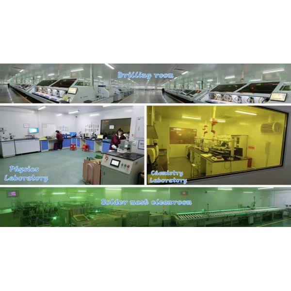
Factory showcase
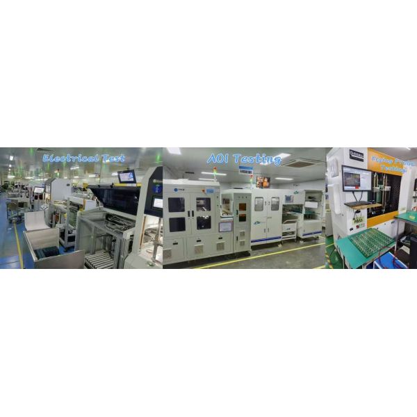
PCB Quality Testing
Certificates and Honors


|
 Custom FR4 Double PCB with Free DFM Check, ISO9001 Certified Manufacturing Service
100% E Test Custom Double Sided Printed Circuit Board Ideal for Electronic Applications
Customized Panelization Double Sided FR4 PCB with ENIG Surface for Consumer Electronics
Custom 2 Layer PCB FR-4 1oz Copper Gold Fingers for Energy Storage with HASL/ENIG Option
Double Sided Blue Oil Half Hole Plate PCB FR4 Material Customized Board
Blue Oil Double Sided Printed Circuit Board FR4 Subtrate Customized Dimension
Custom Double Layer PCB RoHS Certified Black Oil for Medical Equipment Circuit Board
Black Oil Spray Tin Double Panel PCB HASL Treatment Customized Panel Thickness
Red Oil Double Sided PCB Board OSP Surface Treatment Optional Thickness
OSP Halogen Free 2 Layer PCB Board Flame Retardant Double Sided Circuit Board
Custom FR4 Double PCB with Free DFM Check, ISO9001 Certified Manufacturing Service
100% E Test Custom Double Sided Printed Circuit Board Ideal for Electronic Applications
Customized Panelization Double Sided FR4 PCB with ENIG Surface for Consumer Electronics
Custom 2 Layer PCB FR-4 1oz Copper Gold Fingers for Energy Storage with HASL/ENIG Option
Double Sided Blue Oil Half Hole Plate PCB FR4 Material Customized Board
Blue Oil Double Sided Printed Circuit Board FR4 Subtrate Customized Dimension
Custom Double Layer PCB RoHS Certified Black Oil for Medical Equipment Circuit Board
Black Oil Spray Tin Double Panel PCB HASL Treatment Customized Panel Thickness
Red Oil Double Sided PCB Board OSP Surface Treatment Optional Thickness
OSP Halogen Free 2 Layer PCB Board Flame Retardant Double Sided Circuit Board

